
A Hardware-Oriented Echo State Network and its FPGA Implementation
- DOI
- 10.2991/jrnal.k.200512.012How to use a DOI?
- Keywords
- Reservoir computing; echo state network; field programmable gate array
- Abstract
This paper proposes implementation of an Echo State Network (ESN) to Field Programmable Gate Array (FPGA). The proposed method is able to reduce hardware resources by using fixed-point operation, quantization of weights, which includes accumulate operations and efficient dataflow modules. The performance of the designed circuit is verified via experiments including prediction of sine and cosine waves. Experimental result shows that the proposed circuit supports to 200 MHz of operation frequency and facilitates faster computing of the ESN algorithm compared with a central processing unit.
- Copyright
- © 2020 The Authors. Published by Atlantis Press SARL.
- Open Access
- This is an open access article distributed under the CC BY-NC 4.0 license (http://creativecommons.org/licenses/by-nc/4.0/).
1. INTRODUCTION
Neural networks are highly expected to be applied into embedded systems such as robots and automobiles. However, Deep Neural Networks (DNNs) [1] require high computational power because a lot of accumulate operations are being processed using them. Generally, graphics processing units are used to accelerate these computations; however, as their power consumption is high, implementing embedded systems using them is difficult due to a power limit. To mitigate this problem, we have implemented DNNs into hardware such as Field Programmable Gate Arrays (FPGAs), realizing high-speed calculation with low power consumption.
In this paper, we have implemented an Echo State Network (ESN) [2], a kind of Reservoir Computing (RC) into an FPGA. An RC is a Recurrent Neural Network (RNN) model in which only the weights of an output layer are defined in the training step. ESNs are able to learn time-series data faster than general RNNs such as Long Short-term Memory (LSTM). In ESNs, a lot of accumulate operations of input data and weights are executed, however, there are limitations of FPGA resources such as Loot Up Table (LUT), Flip Flop (FF) and Digital Signal Processor (DSP). As a result, we have modified the algorithms and architectures of ESNs. Furthermore, we implement the proposed hardware-oriented algorithms into the FPGA and show the effectiveness of the proposed methods by comparing the proposed circuit with other.
2. ECHO STATE NETWORK
The ESN is a type of RC which consists of three layers: an input layer, a reservoir layer and an output layer, shown in Figure 1, in which the neurons of the reservoir layer are randomly connected to each other.
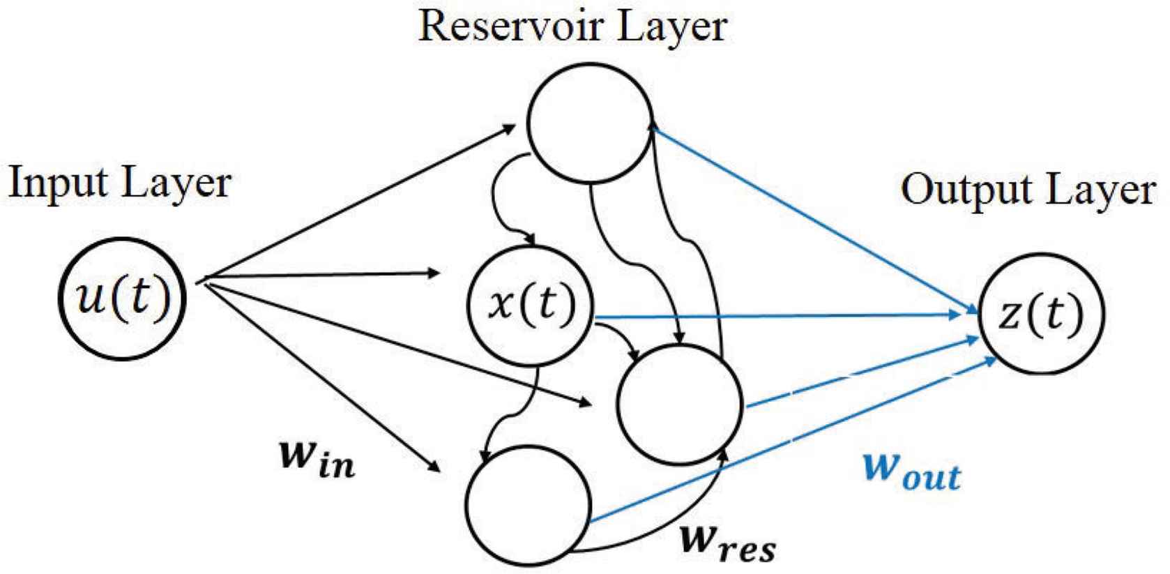
Echo state network.
ESN is described by Equations (1) and (2),
- 1.
All weights of the reservoir layer are generated from a normal distribution.
- 2.
A spectral radius (the maximum eigenvalue of the weights) is calculated and all the generated weights are divided by it.
- 3.
All weights are multiplied by a constant value.
In standard RNNs, all weights are updated following the backpropagation through time algorithm [4]. On the other hand, in the ESN, only the weights of the output layer are updated in one-shot learning through ridge regression as follows:
3. HARDWARE-ORIENTED ESN
There are certain limitations of FPGA’s resources, therefore, we have to modify the algorithms to suitable for FPGA implementation. In this paper, we design a circuit for the ESN by following three methods.
3.1. Quantization
One way to reduce the complexity of a circuit is using quantized values that are able to simplify the computation while maintaining its accuracy [5].
Therefore, we calculated the outputs of the reservoir layer [Equation (1)] using quantized weights. Generally, the weights of input and reservoir layers are real numbers resulting in several DSPs to compute real number multiplications. Therefore, we transformed the real valued weights to ternary values: 0 or ±1. Furthermore, the accuracy by using this quantization for both training and prediction mode are maintained.
The circuit of the neuron is shown in Figure 2. Where n is the number of reservoir’s neurons. un and wn are inputs and weights of input and reservoir layers, respectively, and m is the bit width of the input data. Furthermore, the circuit is able to calculate accumulate operations using only AND and OR operations.
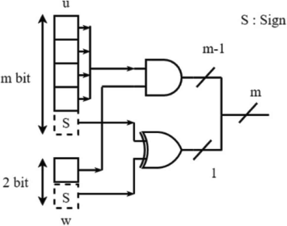
Circuit of neuron.
We have verified the accuracy of a quantized model and the conventional model. The task carried out to evaluate their performance was NARMA10 [6] with equations as follows:
Figure 3 shows the prediction of 100–200 time steps of the quantized model where the number of reservoir neurons was 1000. The black line represents the supervised signal and the blue line represents output of the quantized model. The quantized model was able to reproduce NARMA10. Figure 4 shows the MSE of the supervised signal and outputs of each model, with varying in the number of neurons in the reservoir. The accuracy of the quantized model was similar to conventional model.
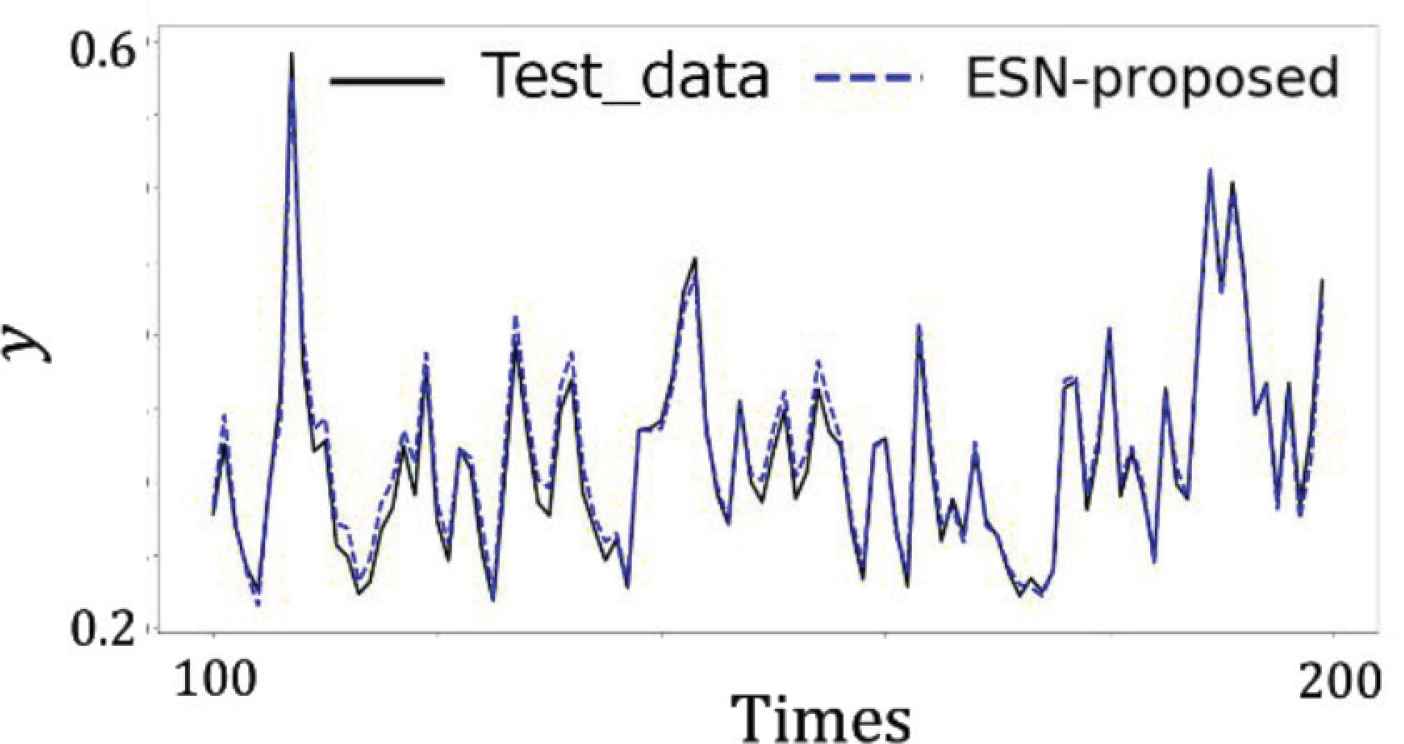
Output of quantized model.
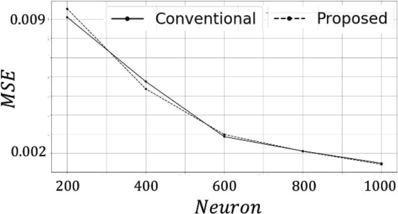
MSE of each model.
3.2. Fixed Point
Generally, computations are conducted with floating point numbers, which are an exponential representation, and can represent a wide range of numbers. A circuit using floating point numbers is more complex as it requires many FPGA resources. In contrast, although the fixed-point representation can only represent a narrow range of numbers, the circuit resources is less complex compared with that using the floating point.
3.3. Sequence Product–Sum of Output Layer
As shown in Figure 5, general product–sum operations can be represented by a tree structure. Using this representation, the number of adders and multipliers increases with the number of neurons. Therefore, in this research, we sequentially calculated the product–sum of the output layer. Figure 6 illustrates the product–sum operation by the proposed method, where Ai is an intermediate variable that temporarily stores the accumulate value. As this method consists of only a single adder, multiplier, and register per neuron in the output layer, the complexity of the circuit is reduced.
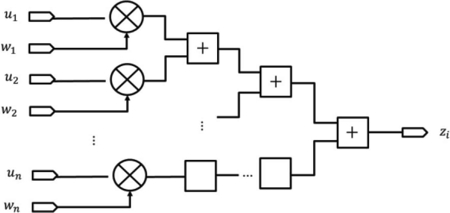
Tree structure of the product–sum circuit.
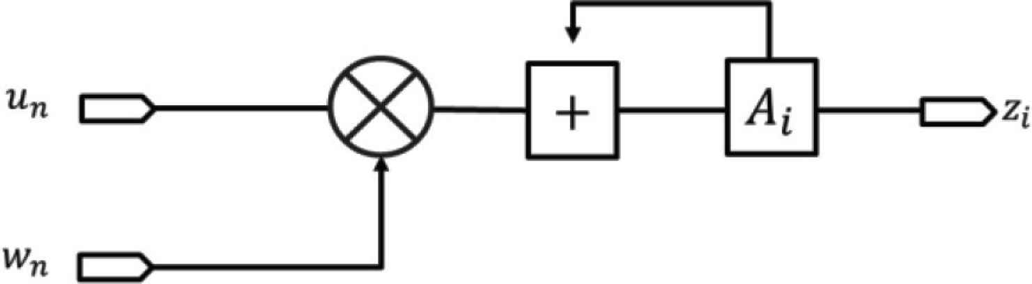
Sequence structure of the product–sum circuit.
4. FPGA IMPLEMENTATION
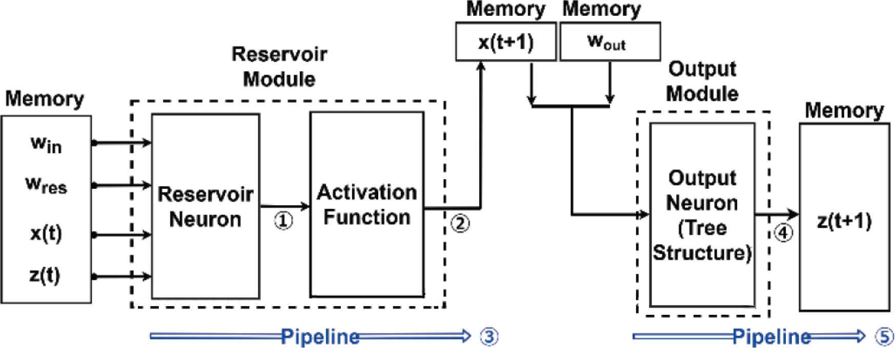
As shown in Figure 7, the conventional model used two pipeline. In process 1 and 2, the reservoir module calculates the state of a single neuron in reservoir layer and stores it in memory. In process 3, the reservoir module repeats the process 1 and 2 for the rest of reservoir neurons. In process 4, an output module calculates the output of a single neuron in output layer by using tree structure. In process 5, the output module repeats process 4 for the rest of output neurons.
Circuits architecture of conventional model.
Figure 8 illustrates the circuits architecture of the proposed model. We implement the sequential structure of the product–sum circuit (as in Figure 6) in parallel for the output layer. Therefore, the proposed circuit is able to calculate a single neuron of reservoir layer and output layer simultaneously in process 4. As a result, the proposed model processes more efficiency than the conventional model. Table 1 shows the comparison between the conventional model and the proposed model.

Circuits architecture of proposed model.
| Operation | Weights of input and reservoir layers | Module of output layer | |
|---|---|---|---|
| Conventional | Floating point | Real values | Tree structure |
| Proposed | Fixed point | Ternary values | Sequence structure |
Details of each circuit
5. EXPERIMENT
In the experiment, we have created two types of circuits in order to verify the effectiveness of the proposed circuit and compared its calculation speed with those of the other devices. The task to evaluate their performance is the prediction problem of sine and cosine waves. The number of neurons in the input, reservoir and the output layers were 2, 100, and 2, respectively, and the prediction was computed in an FPGA. The target device is a Zynq UltraScale+ MPSoC ZCU102. Furthermore, the experiment was conducted with an operating frequency of 200 MHz and a data width of 32-bits operations [7]. Table 2 shows experimental conditions.
| Tool | SDSoC 2018.3 |
|---|---|
| Target device | Zynq UltraScale+ MPSoC ZCU102 |
| Clock frequency | 200 MHz |
Experimental conditions
6. RESULTS
Figure 9 shows the prediction of the conventional and proposed circuits. The black, blue, and red lines represent the supervised signal, prediction of the conventional circuit and prediction of the proposed circuit, respectively. Both circuits were able to reproduce sine and cosine waves. Tables 3 and 4 shows the utilization of resources for the conventional and proposed circuit, respectively. The proposed method was able to reduce the overall use of resources approximately 50%. Table 5 shows the comparison between electric energy of conventional circuit and proposed circuit. The proposed method reduced the electric energy consumption by approximately 80% compared with the conventional one. Table 6 shows a comparison between the computation speed of the FPGA and other devices. The proposed circuit was approximately 25 and 340 times faster than a desktop CPU and embedded CPU, respectively.
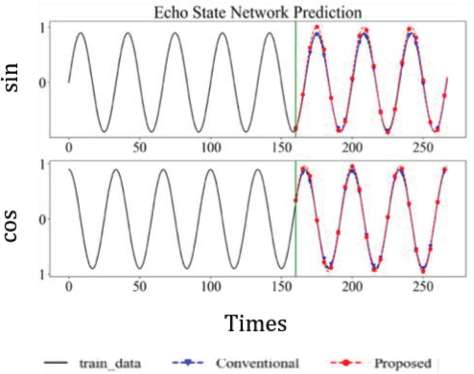
Output of circuits.
| Used | Total | Utilization | |
|---|---|---|---|
| BRAM_18k | 106 | 912 | 11.57 |
| DSP_48E | 519 | 2520 | 20.48 |
| LUT | 60557 | 274,080 | 22.07 |
| FF | 96556 | 548,160 | 17.55 |
Utilization of resources for the conventional circuit
| Used | Total | Utilization | |
|---|---|---|---|
| BRAM_18k | 48 | 912 | 5.26 |
| DSP_48E | 20 | 2520 | 0.79 |
| LUT | 28933 | 274,080 | 10.56 |
| FF | 44021 | 548,160 | 8.03 |
Utilization of resources for the proposed circuit
| Latency (ms) | Power (w) | Electric energy (w*ms) | |
|---|---|---|---|
| Conventional | 0.43 | 1.46 | 0.63 |
| Proposed | 0.20 | 0.67 | 0.13 |
Electric energy consumption of each circuits
| Platform | Latency (ms) |
|---|---|
| CPU 3.2GHz (i7-8700) | 5.215 |
| Embedded CPU 1.2GHz (Quad Arm Cortex-A53) | 68.123 |
| FPGA 200MHz (XCZU9EG-2FFVBG1156E) | 0.200 |
Computation speed of devices
7. CONCLUSION
We were able to successfully adapt the circuit to enhance ESN computation in the FPGA. As a result, high-speed computation was possible while the circuit resources were reduced. To achieve this, fixed-point computation, quantification of weights, and sequential product–sum computation techniques were used.
In the future, it is expected to apply the proposed circuit and methods to embedded systems such as automobiles and robots.
CONFLICTS OF INTEREST
The authors declare they have no conflicts of interest.
ACKNOWLEDGMENT
This research is supported by
AUTHORS INTRODUCTION
Mr. Kentaro Honda
 He received Master of Engineering degree from Kyushu Institute of Technology in 2019. His research interests include neural network and digital circuit.
Associate Prof. Hakaru Tamukoh
 He received the B.Eng. degree from Miyazaki University, Japan, in 2001. He received the M.Eng. and the PhD degree from Kyushu Institute of Technology, Japan, in 2003 and 2006, respectively. He was a postdoctoral research fellow of 21st century center of excellent program at Kyushu Institute of Technology, from April 2006 to September 2007. He was an Assistant Professor of Tokyo University of Agriculture and Technology, from October 2007 to January 2013. He is currently an Associate Professor in the Graduate School of Life Science and System Engineering, Kyushu Institute of Technology, Japan. His research interest includes hardware/software complex system, digital hardware design, neural networks, soft-computing and home service robots. He is a member of IEICE, SOFT, JNNS, IEEE, JSAI and RSJ.
REFERENCES
Cite this article
TY  - JOUR
AU  - Kentaro Honda
AU  - Hakaru Tamukoh
PY  - 2020
DA  - 2020/05/18
TI  - A Hardware-Oriented Echo State Network and its FPGA Implementation
JO  - Journal of Robotics, Networking and Artificial Life
SP  - 58
EP  - 62
VL  - 7
IS  - 1
SN  - 2352-6386
UR  - https://doi.org/10.2991/jrnal.k.200512.012
DO  - 10.2991/jrnal.k.200512.012
ID  - Honda2020
ER  -